One of the ways to satisfy the emerging need for sustainable energy sources is via the production of large-scale, cheap and easy-to-process solar cells. This has made the development of organic photovoltaic devices (OPVs) based on carbon based semiconductors (conjugated polymers and small molecules) an exciting and rapidly growing field of research and technology. These materials are efficient light absorbers and their properties can be tuned through chemical synthesis. Furthermore, the fabrication of complete solar cells can be done almost entirely from solution using scalable processing methods such as offset printing. The power conversion efficiency (PCE) of OPVs has increased substantially in the past two decades, with values of 9 - 11% now being attained for laboratory scale single and tandem-junction devices. These promising figures of merit have resulted from the joint development of novel organic semiconductors and device architectures that are optimised for efficient light harvesting.
Our goal in the Optoelectronics Group is to develop new approaches for improving solar cell efficiencies. For OPVs, this includes the development and characterisation of novel materials and device architectures. We also investigate the fundamental aspects of photocurrent generation in these systems using state-of-the-art optical spectroscopy techniques, exploring phenomena such as excited state delocalization, coherence and also Singlet fission on timescales as short as ~ 30fs.
Organic Photovoltaic Devices
A typical OPV has a layered structure involving: a substrate, transparent bottom electrode, photoactive layer and top metal electrode (fig. 1). Light is converted to electrical current in the photoactive layer, which has a typical thickness of ~ 100 nm. In efficient OPVs, this layer is a composite of two or more semiconductors (electron donors and acceptors) mixed together to form a nanostructured (or bulk) heterojunction for charge generation.
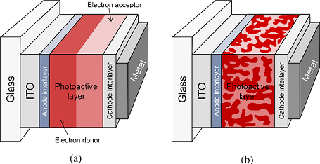
Figure 1. Schematic illustration of the different layers present in organic photovoltaic devices. The photoactive layer is characterised by a planar structure in part (a), where a single heterojunction interface is present between the electron donor and electron acceptor. In part (b) the electron donor and acceptor are blended together at the nanoscale. As a consequence, heterojunction interfaces exist throughout the bulk of the photoactive layer (the so-called ‘bulk-heterojunction’ architecture)
Photocurrent generation in OPVs is a multistep process that can be summarised as follows. Initially, photon absorption by a molecule in the active layer promotes an electron to an excited state, resulting in a localised and tightly bound electron-hole pair (a so-called molecular exciton). To contribute to the photocurrent from the solar cell, the exciton must be dissociated, which requires the coulomb interaction between the hole and electron (~ 0.5 eV) to be overcome. This step can occur at an interface between electron accepting and donating semiconductors, resulting in the transient formation of a charge-transfer state whereby the electron and hole exist on different molecules. The dissociation of the charge-transfer state is then followed by (1) charge transport - where electrons and holes ‘hop’ between adjacent electron acceptor and donor molecules respectively – and (2) charge extraction at the electrodes of the solar cell. For efficient overall performance, all of these steps should be well characterised and carefully optimized.
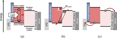
Figure 2. The energy diagram of typical organic solar cell and different stages of the photocurrent generation process (a) exciton generation, (b) charge transfer state dissociation, (c) charge transport and extraction.
Examples of recent OPV projects
-
Energy Level Cascades
We have recently designed an energy cascading structure in a polymer:polymer photovoltaic devices to suppress recombination and improve quantum yields. By inserting a thin polymer interlayer with intermediate energy levels, and/or a high dielectric constant, electrons and holes can be effectively decoupled. This allows charges to move away from each other while being spatially separated from recombination. An increase in open-circuit voltage and short-circuit current are observed in modified devices.
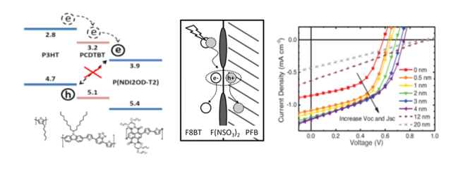
Figure 3. The concepts of charge-transfer cascade [1] and polyelectrolyte recombination-blocking layer [2] in OPV. Right figure shows the OPV performance improvement as a function of interlayer thickness.
[1]. Tan Z.-K., Johnson K., Vaynzof Y., Bakulin A.A., Chua L.-L., Ho P.K.H., Friend R.H., Suppressing Recombination in Polymer Photovoltaic Devices via Energy-Level Cascades, Adv. Mater., 25, 4131 (2013)
[2]. Kumar A., Pace G., Bakulin A.A., Fang J., Ho P.K.H., Huck W.T.S., Friend R.H., Greenham N.C., Donor–Acceptor Interface Modification by Zwitterionic Conjugated Polyelectrolytes in Polymer Photovoltaics, Energy Environ. Sci., 6, 1589 (2013)
-
Resolving charge extraction via transient absorption spectrosocpy
One of the loss mechanisms in OPV devices is the recombination of electrons and holes prior to charge extraction. Convetionally, this recombination process is thought to be dominated by the bulk photoactive layer (e.g. an inappropriate donor:acceptor nanostructure). We have shown that the photoactive layer / electrode interface also has a strong influence on the time spent by mobile charges within the device [3]. Transient absorption spectroscopy is an ideal tool with which to probe charge carrier dynamics, from generation and extraction, owing to the relatvely strong absorption of infra-red light by hole polarons. Modifying this interface (for example, via the insertion of a thin conjugated polymer electrolyte layer at the electrode, or spin-coating a neat polar solvent onto the photoactive layer) permits charges to leave the device much faster than in reference devices.
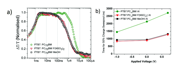
Figure 4: (a) Normalised kinetics for holes in operating devices measured in situ via TA spectroscopy at short-circuit: reference PTB7:PC70BM device with no modification (green circles); a device modified with 2 nm F(NSO3)2 (red triangles); and a device modified with methanol (black squares). (b) The time measured from TA kinetics to extract 50% of photogenerated charges out of the device under various applied voltages.
[3] Kumar A., Lakhwani G., Elmalem E., Huck W.T.S, Rao A., Greenham N.C., Friend R.H., Interface limited charge extraction and recombination in organic photovoltaics, Energy Environ. Sci., 7, 2227 (2014)
-
Evaluating OPV stability through atmospheric testing
Stability is a current bottleneck in the realisation of efficient & practical OPV devices, with many solar cells undergoing a significant ‘burn-in’ phase where performance undergoes a relatively rapid drop before stabilising. Minimising this reduction requires a thorough understanding of the intrinsic and extrinsic factors that influence burn-in behaviour, as well as its effects. We have recently developed a state-of-the-art setup for characterising device stability under controlled atmospheres, permitting the effects of water- and oxygen-induced degradation to be studied separately. Unique to our setup is the inclusion of transient photocurrent and photovoltage technqiues, allowing us to track the dynamics of charge transport and recombination in-situ to the degradation process, complementing conventional measurements of power conversion efficiency. This setup has previously been used to characterise the stability of PbSe nanocrystal photovoltaic cells [4], with current work focussing on OPVs using derivtaives of the low bandgap polymer PTB7.
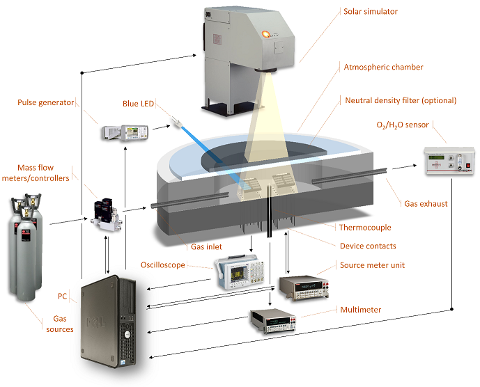
Figure 5: Schematic of the degradation setup with principle components identified (figure credit: Konrad Domanski).
[4] Asil D., Walker B.J., Ehrler B., Vaynzof Y., Sepe A., Bayliss S., Sadhanala A., Chow P.C.Y., Hopkinson P.E., Steiner U., Greenham N.C., Friend R.H., Role of PbSe Structural Stabilization in Photovoltaic Cells, Adv. Funct. Mater., 25, 928 (2015)