For elemental and crystalline semiconductors, the arrangement of elements in the lattice gives rise to delocalised electronic states and band structure. The quality of the band structure is therefore highly sensitive to defects (such as impurities and crystallite boundaries) meaning that creating high-performance materials by this approach is an intrinsically expensive process. The primary brake on uptake of cheap, large area photovoltaics and circuitry for the last several decades has been the relatively high cost of silicon crystal, which must be processed from a purified melt at extremely high temperature. Even higher costs are associated with luminescent semiconductor crystals for LEDs.
An alternative approach is to utilise materials in which semiconducting behaviour is intrinsic, rather than an emergent property of the lattice. Molecular semiconductors are one such class of material, whereby synthetic molecules with desirable electronic structure are used to form the active layer of an optoelectronic device. The electronic properties of molecular semiconductors are largely ‘hard-wired’ into each molecule, and do not rely on a particular crystal structure being formed. This renders them significantly more tolerant to impurities, packing defects or grain boundary effects and so allows far greater scope for low-cost processing. Decoupling electronic and physical structure also casts bandgap engineering as a problem of molecular design, rather than crystal composition, which makes it accessible to the vast field of synthetic chemistry. In particular, the tremendous flexibility of organic (carbon-based) chemistry has led to the dominance of organic molecules within molecular semiconductor technology.
· Chemistry and conjugation
Semiconducting and metallic organic materials are based on chains and sheets of sp2-hybridised carbon. Neutral atomic carbon contains six electrons, two tightly bound in 1s orbitals and four valence electrons in a 2s2, 2p2 configuration. However, in a carbon-based molecule the total bond energy may be reduced by the formation of ‘sp’ hybrid states between the filled 2s- and partially filled 2p-shells. Three primary hybrid states are possible: tetrahedrally aligned sp3 orbitals, planar hexagonal sp2 orbitals and linear sp orbitals. Figure 1 shows examples of all these configurations.
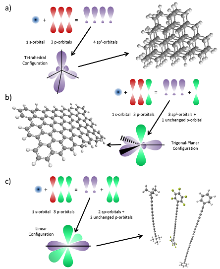
Figure 1 Schematics of the electronic orbitals of a) sp3 hybridisation (diamond), b) sp2 hybridisation (graphene) and c) sp hybridisation (heptayne, octayne and dodecayne linear acetylenic carbon, with various capping groups)
Since only three of the four valence electrons hybridise in the sp2 configuration, the final electron occupies a perpendicular 2pz orbital. The sharing of sp orbitals between adjacent carbons leads to strong, highly directional ‘σ-bonding’, which allows the formation of stable carbon chains, sheets and branched structures.
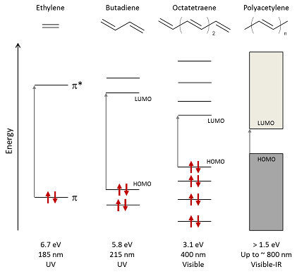
Figure 2 Schematic of energy-level splitting and absorption in alkenes with increasing conjugation length, highlighting the lowest-energy optical transitions from HOMO to LUMO. The bandgap of polyacetylene depends on both the number of monomers n and the effective conjugation length in the polymer. Arrows represent spin-paired electrons.
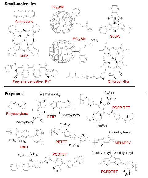
Figure 3 Chemical structures for a range of commonly used small-molecule and polymer semiconductors. CuPc = Copper phthalocyanine, SubPc = boron subphthalocyanine chloride.
Hybridisation between the remaining 2pz orbitals gives rise to weaker π (bonding) or π* (anti-bonding) orbitals. These planarise the molecule, which allows delocalisation of π/π*-states over many carbon atoms—a process known as conjugation. In the symmetric (π) configuration, significant electron density is present between neighbouring carbon atoms, stabilising this configuration compared with the anti-symmetric (π*) one. In a simple two-carbon system, the two unpaired 2pz electrons will therefore tend to occupy the two spin-allowed π states, leaving the unoccupied π* states above a forbidden energy gap Eg: the difference between the highest occupied molecular orbital (HOMO) and lowest unoccupied molecular orbital (LUMO) which is analogous to the bandgap in a crystalline material. sp2-hybridised molecules can therefore act as semiconductorsd
Increasing the conjugation length has the effect of broadening the ensemble of hybrid states into a quasi-continuous ‘band’ and narrowing this gap: for example, controlling the degree of polymerisation of ethylene can vary Eg from 6.7 eV for the monomer to around 1.5 eV for stretch-oriented polyacetylene (with effective conjugation over more than 20 carbon atoms) as illustrated in Fig. 2.
A similar effect occurs when the π orbitals of neighbouring molecules overlap to allow delocalisation over several molecular layers. Such ‘π–π stacking’ is important for transport and also leads to a lower optical bandgap. A combination of intra- and inter-molecular delocalisation, along with the numerous other routes which exist for engineering the HOMO–LUMO offset, can therefore lead to molecules with very strong absorption/emission in the visible spectral range, suitable for LEDs and photovoltaics. A selection of such molecules is shown in Fig. 3.
Organic materials have a number of properties which distinguish them from crystalline materials and have profound consequences for their physics:
-
Organic semiconductors are low dielectric constant (e) materials
For example, epentacene ~ 4, ePPV ~ 2 whereas eSi ~ 12, eGaAs ~ 13. In materials with high e, dielectric screening reduces the Coulomb attraction between excited electron-hole pairs to a few 10s of meV. Such weakly bound e-h pairs (Wannier-Mott excitons) therefore undergo spontaneous dissociation into free charges via interactions with room-temperature lattice phonons. In materials with low e, the Coulomb attraction is not strongly screened, leading to Frenkel-type excitons with binding energies around 0.1–1 eV. Dissociation of these excitons into free charge carriers is rarely spontaneous at room temperature (problematic for photovoltaics, potentially good for LEDs). If they do not dissociate, excitons in organic materials typically exhibit luminescence lifetimes of a few nanoseconds.
-
Organic materials are electronically ‘soft’
Charge carriers moving through an organic material are usually localised to a few carbon atoms, and so act as large perturbations to the local electronic structure. Polarisation of the local medium (enhanced by low e) and the breaking of local conjugation leads to geometric relaxation of the molecule. The fundamental charge carrier in organic materials is thus a polaron, a quasiparticle comprising the charge self-localised by its associated molecular distortion. Migration of polarons between polymer chains or conjugated regions involves significant reorganisation energy, reducing mobility. Depending on how stiff a molecule is, geometric relaxation can also produce a significant Stokes’ shift between absorption and emission spectra, which is particularly beneficial for reducing self-absorption in organic LEDs.
-
Transport of carriers is limited by “hopping” between molecules
Since organic molecules (and particularly polymers) typically exhibit low symmetry, transport can be highly anisotropic. For a stiff conjugated polymer, intra-chain transport will be faster than transport in the π–π stacking direction, while lateral transport through saturated side-groups can be very poor. Intra-chain hole mobilities as high as 600 cm2/Vs have been reported for ladder-type poly(p-phenylene), whereas measured mobilities are of order 1–10 cm2/Vs in solid films, and depend strongly on polymer orientation. Such transport also depends on temperature and electronic disorder since each inter-molecular “hop” requires significant molecular reorganisation. Such disorder also limits the diffusion rate for excitons, by limiting the number of nearby sites which are energetically accessible.
-
Organic semiconductors are easy to deposit
Small organic molecules may be sublimed under vacuum at relatively low temperature, enabling the creation of well-defined films and layer structures without the need for high-temperature, high-purity processing. Solubility can also be specifically designed into the molecule without significantly affecting its electronic structure, usually achieved by attaching flexible saturated side groups along the main backbone (examples are shown in figure 4). Many organic molecules can therefore be formed into inks and processed from solution. As solid films, these soluble semiconductors are typically flexible and highly resistant to fracture, lending the collection of technologies which exploit them the umbrella term ‘plastic electronics’.
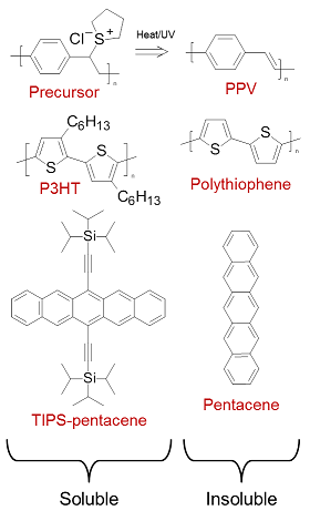
Figure 4 Typical routes to solubilisation. Insoluble poly(p-phenylenevinylene) (PPV) is formed in situ from a soluble precursor via a leaving-group reaction. Insoluble polythiophene and pentacene are rendered soluble by the inclusion of flexible side chains.
Deposition of organic semiconductors from solution can take advantage of the wide range of thin-film coating technologies already employed by existing industries. These include inkjet and screen printing for individual substrates and extend to continuous roll-to-roll manufacture, for example using slot-die, gravure printing or doctor-blading (see Fig. 5). The existence of mature, low-cost, large-area manufacturing routes means that scaling-up of organic semiconductor technology is widely expected to be a relatively cheap process, if the materials set can also reach maturity.
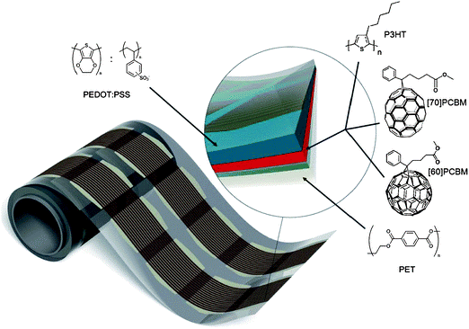
Figure 5 A roll of printed OPV modules produced in a continuous R2R process. The inset shows the layer stack, comprising PET-ITO-ZnO-P3HT:PCBM-PEDOT:PSS-printed silver paint and encapsulated using roll-to-roll lamination post production. Reproduced from Krebs et al. (2010).